- 您现在的位置:买卖IC网 > Sheet目录337 > LE25U20AMB-AH (ON Semiconductor)IC MEM 2MBIT SERIAL FLASH 8SOP
�� �
�
�LE25U20AMB�
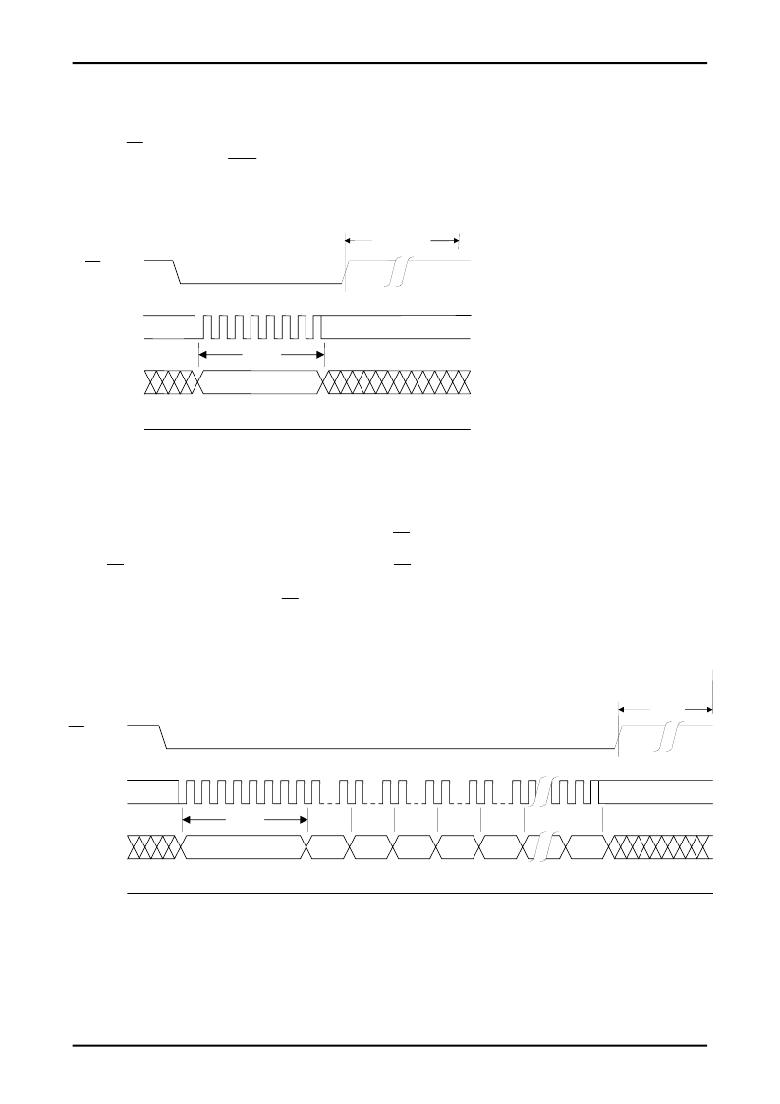
�8.� Chip� Erase�
�Chip� erase� is� an� operation� that� sets� the� memory� cell� data� in� all� the� sectors� to� "1".� "Figure� 14� Chip� Erase"� shows� the�
�timing� waveforms,� and� Figure� 21� shows� a� chip� erase� flowchart.� The� chip� erase� command� consists� only� of� the� first� bus�
�cycle,� and� it� is� initiated� by� inputting� (C7h).� After� the� command� has� been� input,� the� internal� erase� operation� starts� from�
�the� rising� CS� edge,� and� it� ends� automatically� by� the� control� exercised� by� the� internal� timer.� Erase� end� can� also� be�
�detected� using� status� register� RDY.�
�Figure� 14� Chip� Erase�
�Self-timed�
�Erase� Cycle�
�tCHE�
�CS�
�Mode3�
�0� 1� 2� 3� 4� 5� 6� 7�
�SCK�
�Mode0�
�8CLK�
�SI�
�SO�
�C7h�
�High� Impedance�
�9.� Page� Program�
�Page� program� is� an� operation� that� programs� any� number� of� bytes� from� 1� to� 256� bytes� within� the� same� sector� page� (page�
�addresses:� A17� to� A8).� Before� initiating� page� program,� the� data� on� the� page� concerned� must� be� erased� using� small�
�sector� erase,� sector� erase,� or� chip� erase.� "Figure� 15� Page� Program"� shows� the� page� program� timing� waveforms,� and�
�Figure� 22� shows� a� page� program� flowchart.� After� the� falling� CS,� edge,� the� command� (02H)� is� input� followed� by� the�
�24-bit� addresses.� Addresses� A17� to� A0� are� valid.� The� program� data� is� then� loaded� at� each� rising� clock� edge� until� the�
�rising� CS� edge,� and� data� loading� is� continued� until� the� rising� CS� edge.� If� the� data� loaded� has� exceeded� 256� bytes,� the�
�256� bytes� loaded� last� are� programmed.� Th� e� program� data� must� be� loaded� in� 1-byte� increments,� and� the� program�
�operation� is� not� performed� at� the� rising� CS� edge� occurring� at� any� other� timing.� The� page� program� time� is� 2.0ms� (typ.)�
�when� 256� bytes� (1� page)� are� programmed� at� one� time.�
�Figure� 15� Page� Program�
�Self-timed�
�Program� Cycle�
�tPP�
�CS�
�Mode3�
�0� 1� 2� 3� 4� 5� 6� 7� 8�
�15� 16�
�23� 24�
�31� 32�
�39� 40�
�47�
�2079�
�SCK�
�Mode0�
�8CLK�
�SI�
�02h�
�Add.�
�Add.�
�Add.�
�PD�
�PD�
�PD�
�SO�
�High� Impedance�
�No.A2097-12/21�
�发布紧急采购,3分钟左右您将得到回复。
相关PDF资料
LFDAS12XSIT
HARDWARE MC9S12XS 112-PIN
LFXP10E-L-EV
BOARD EVAL LATTICEXP10E STD
LH28F008SCHT-TE
IC FLASH 8MBIT 85NS 40TSOP
LH28F160S3HNS-TV
IC FLASH 16MBIT 100NS 56SSOP
LH28F160S5HNS-S1
IC FLASH 16MBIT 70NS 56SSOP
LH28F320S3HNS-ZM
IC FLASH 32MBIT 110NS 56SSOP
LH28F320SKTD-ZR
IC FLASH 32MBIT 70NS 48TSOP
LHF00L28
IC FLASH 16MBIT 70NS 48TSOP
相关代理商/技术参数
LE25U20AMBM02-AH
功能描述:闪存 RoHS:否 制造商:ON Semiconductor 数据总线宽度:1 bit 存储类型:Flash 存储容量:2 MB 结构:256 K x 8 定时类型: 接口类型:SPI 访问时间: 电源电压-最大:3.6 V 电源电压-最小:2.3 V 最大工作电流:15 mA 工作温度:- 40 C to + 85 C 安装风格:SMD/SMT 封装 / 箱体: 封装:Reel
LE25U40CFQ-AH
制造商:ON Semiconductor 功能描述:REEL / S-FLASH MEMORY(4M)
LE25U40CMC
制造商:SANYO 制造商全称:Sanyo Semicon Device 功能描述:4M-bit (512K??8) Serial Flash Memory
LE25U40CMC-AH
功能描述:闪存 S-FLASH MEMORY(4M)
RoHS:否 制造商:ON Semiconductor 数据总线宽度:1 bit 存储类型:Flash 存储容量:2 MB 结构:256 K x 8 定时类型: 接口类型:SPI 访问时间: 电源电压-最大:3.6 V 电源电压-最小:2.3 V 最大工作电流:15 mA 工作温度:- 40 C to + 85 C 安装风格:SMD/SMT 封装 / 箱体: 封装:Reel
LE25U40CMCQ00-AH
制造商:ON Semiconductor 功能描述:Flash S-FLASH MEMORY(4M)
LE25U40CQE
制造商:SANYO 制造商全称:Sanyo Semicon Device 功能描述:4M-bit (512K??′8) Serial Flash Memory
LE25U40CQE-AH
功能描述:电可擦除可编程只读存储器 RoHS:否 制造商:Atmel 存储容量:2 Kbit 组织:256 B x 8 数据保留:100 yr 最大时钟频率:1000 KHz 最大工作电流:6 uA 工作电源电压:1.7 V to 5.5 V 最大工作温度:+ 85 C 安装风格:SMD/SMT 封装 / 箱体:SOIC-8
LE25U40CQES00-AH
制造商:ON Semiconductor 功能描述:S-FLASH MEMORY(4M)